Jerrold A. Floro

About
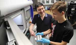
My passion in research is to investigate and exploit nanoscale self-assembly and pattern formation in inorganic materials, to enhance properties and develop material functionality. My group employs a range of techniques to synthesize materials, including vapor phase thin film growth, laser processing, melting and rapid solidification (including additive manufacturing), powder processing, and solid-state phase transformations. There is plenty of room at the bottom -- and there is both beauty and mystery there as well.
Bio: I earned my Bachelor's degree in Physics at Colorado State University in 1983, where I did research on modification of surfaces using low energy ion beams, including a project that was likely producing carbon nanotubes before they were "a thing". I then joined the IBM Thomas J. Watson Research Center in Yorktown Heights, NY, where I learned multiple thin film deposition techniques, materials characterization, vacuum technology, and got a great exposure to different sorts of research going on at a very vibrant place. I first heard about Materials Science as a field of study here, and then joined MIT's Ph.D. program in MSE in 1986. My thesis research investigated grain growth in thin films driven by anisotropic surface energy and elastic energy. After finishing in 1992, I began a post doc at Sandia National Labs in Albuquerque, NM. Over the next 14 years, I worked on epitaxial and thin film growth sicence, including quantum dot self-assembly in Group IV semiconductors, the origins of residual stresses in thin films, and strain relaxation mechanisms in III-nitride layers and heterostructures. During this time I helped co-invent the multi-beam optical stress sensor and the light-scattering spectrometer, for real-time, in situ investigation of evolving stress and surface morphology during film growth. In 2006, feeling that my strengths were best suited to academia, I joined the faculty of UVa in the Materials Science and Engineering department. My research currently has migrates towards bulk materials processing via rapid solidfication, thermomechanical treatment, powder processing, and/or solid-state phase transformations. I still maintain and use capabilities in thin film growth and processing. These varied approaches are especially useful for new nanoelectronic, thermoelectric and ferromagnetic materials.
Education
Ph.D. Materials Science and Engineering, MIT, 1992
Post-Doc at Sandia National Laboratories, New Mexico, 1992-1994
B.S. Physics, Colorado State University, 1983
Making better materials --> every atom in its place.
