CAREER Award: Seeing the Future
Kyusang Lee Earns Prestigious National Science Foundation Grant to Build the Equivalent of a Human Eye and Its Visual Cortex
How humans see, process visual information and then react to it in a fraction of a millisecond is nothing short of mind-blowing. It’s a biological masterpiece. But can eyesight be replicated for use in machines?
University of Virginia School of Engineering assistant professor Kyusang Lee has earned a CAREER AWARD from the National Science Foundation to research and build the equivalent of a human eye and its visual cortex to be used as optical sensors for autonomous vehicles, robotics, manufacturing processes or surveillance systems.
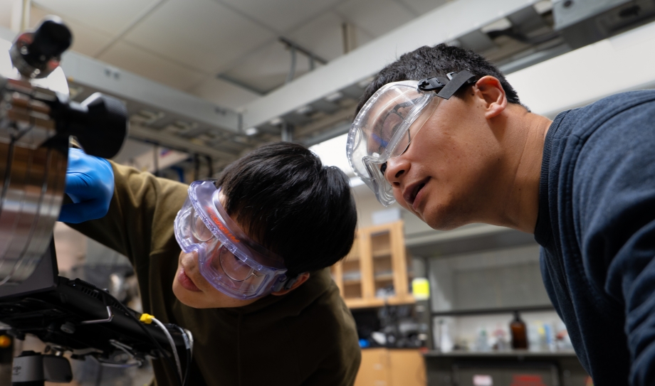
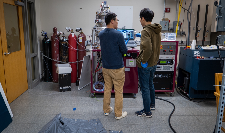
In his lab at UVA, Lee is developing a hemispherical image sensor that mimics the shape of the human eye. He is coupling the sensor with state-of-the-art hardware that will process the input in much the same way human neural synapses process and store visual information in our brains. This serves to both increase the speed at which information can be analyzed and improve energy consumption by many orders of magnitude.
“Current sensor technology consumes a lot of energy and takes in a lot of useless information from the background of a scene. We would like to reduce and pre-process the data at the image sensor itself, filtering the useful information to minimize the burden on the central processing unit. This device promises to be 1,000 times more efficient in computing than current technology,” Lee said.
Lee, who has joint appointments in the Charles L. Brown Department of Electrical and Computer Engineering and the Department of Materials Science and Engineering, came to UVA after his post-doctoral research work concluded at the Massachusetts Institute of Technology in 2017.
While at MIT, Lee collaborated on a project using graphene, basically a one-atom-thick layer of graphite, to copy information from one semiconductor to another, which was a breakthrough in production of semiconductors with the potential not only to improve their operations but make semiconductors much cheaper to produce.
Lee is using the same technology to create his thin-film image sensors. He is growing indium gallium arsenide crystals, known for their image-sensing capabilities, on top of graphene, which is slick and will allow the image sensors to be peeled off in a thin sheet. Because of its pliable form, the sensor can then be assembled as a concave structure like the retina of the human eye.
“One of the issues with a conventional image sensor is that it has a lot of lenses in front of the device because you need to focus the scene onto the sensor. So, an advantage of the hemispherical sensor is that you can simplify the optics into one or two lenses, like we have in the human eye,” Lee said. “And, by curving the sensor, you get a very wide, nearly 180-degree field of view.”
The sensor technology Lee is inventing will also be capable of working in very low light, and in different color spectrums, making it perfect for night vision operations and other situations when light is minimal.
“The combination of an indium gallium arsenide thin film on graphene with device-level optical features to perfect an image sensor is really novel,” said John R. Scully, Charles Henderson Chaired Professor and chair of the Department of Materials Science and Engineering. “It is an ingenious combination of materials science and engineering and electrical and computer engineering sensor technology to produce a potential breakthrough.”
Integrated into Lee’s machine eye is a type of technology that was first theorized by American electrical engineer Leon Chua in 1971 and is only now coming into existence. Chua surmised that the fourth fundamental electrical component, behind the resistor, capacitor and inductor, would be the memristor, a type of non-volatile, electronic memory that can retain its stored memory even without power. More than 40 years went by after Chua postulated the existence of the memristor before the first device was built by Hewlett Packard in 2008. The technology is now in use in applications like voice and facial recognition.
"Memristors are tiny, electronic, non-volatile memory devices that can be used as artificial synapses, and memristor arrays hold great promise for realizing artificial neural networks in hardware,” said Nikolaos Sidiropoulos, Louis T. Rader Professor and chair of the Department of Electrical and Computer Engineering. “Professor Lee is an expert in heterogeneous integration of transistors and memristors, which puts him in a unique position to demonstrate the first miniature visual recognition hardware system."
What makes the memristor so special is that its memory can be programmed, for example to recognize certain features of images, such as shapes and colors.
Memristors naturally use less energy and are much faster than current solid-state memory storage. In effect, these devices emulate the learning and memory storage properties of biological synapses, a trait that makes the technology very attractive to electrical and computer engineers.
A synapse is a junction between a pair of nerve cells. When a nerve impulse reaches that junction at the end of a neuron, it triggers the neuron to release chemical neurotransmitters. The neurotransmitters will then flow into the gap between the neurons and come to rest in the receptor of the other neuron. Once this happens, the chemical signal is converted back into an electrical nerve impulse, and then the process is completed until it ends with some effect. This pipeline of impulses connects a sensory organ to the brain. Many neuroscientists believe that long-term memory is formed in synapses that “learn” a behavior over time or in the creation of new memories.
“A lot of machines already use a type of artificial neural network to recognize things, like Siri or facial recognition. The problem is, the way this process works now, most applications work at the software level instead of using dedicated hardware. That is very energy intensive and takes more time,” Lee said. “Your brain is basically using synapses as memory by way of it being trained. We can now do this at the hardware level. By training this hardware, programming it up front, you can expedite the sensor process, mimicking the synapse of the neuron.”
Lee has already developed a hemispherical image sensor and separately fabricated the artificial synapse. His next step is to integrate the two devices into a single platform, and he expects that process to take a year or so to have a fully functioning prototype. The artificial neural synapse Lee is developing can be applied to many other types of sensors like pressure and temperature sensors, as well as fire detectors and uses in manufacturing.
“I like to create things that can be useful in real life,” Lee said. “I’m working to link science and technology and bringing that into commercialization in order to make it accessible.”