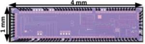
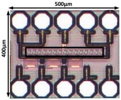
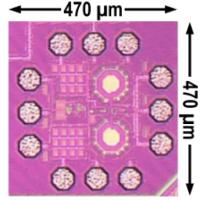
Chip Gallery
Chip Gallery
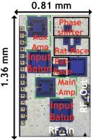
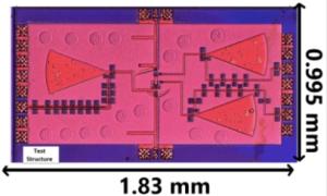
An X-band Phase Noise Canceling Feedforward Amplifier
InP 250nm HBT, 2023
The proposed feedforward amplifier with a noise cancellation scheme achieves more than 16 dBm output power, lower than -155 dBc/Hz additive phase noise at 10 kHz offset from 9.5 GHz carrier while the amplifier is biased in class A operation mode.
Designer(s): Pedram, Samin
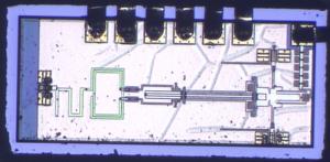
A Terahertz InP HBT Quadrupler
InP 250nm HBT, 2023
The proposed quadrupler operates at 600 GHz.
Designer(s): Vinay, Prerana
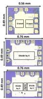
A Low-Additive Phase Noise Low-Power Static Frequency Dividers
InP 250nm HBT, 2023
The proposed static frequency dividers achieve low additive phase noise -143.5 dBc/Hz and -138.2 dBc/Hz for 10 GHz input frequency at 10 kHz offset for synchronous divider by 4 and divider by 2, repectively.
Designer(s): Samin Hanifi
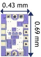
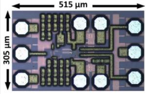
A Wideband Ultra-Low Additive Phase Noise Power Amplifier
InP 250nm HBT, 2023
This is a 250 nm InP heterojunction bipolar transistor (HBT) power amplifier (PA). The proposed PA illustrates -150.0 dBc/Hz additive phase noise at 10 kHz offset from a 10 GHz carrier while drawing 54.4 mA DC current from a 3.1 V collector supply in the compression point; moreover, PA delivers a maximum of 18.1 dBm saturation output power and a peak gain of 16.7 dB at 10 GHz frequency.
Designer(s): Pedram Shirmohammadi
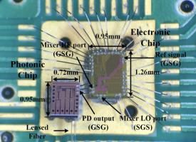
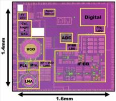
Compact Heterogeneously Integrated Optical Phase-Locked Loop
CMOS 65 nm GP, 2022
This optical phase-locked loop (OPLL) is a heterogeneous integration of a photonic integrated circuit (PIC) and a CMOS electronic integrated circuit (EIC) to achieve a compact size and reduce loop delay. The frequency difference between two lasers is locked continuously from 10 GHz to 40 GHz with a significant improvement in the phase noise from −30 dBc/Hz to −70 dBc/Hz at 100 Hz offset frequency within the loop bandwidth.
Designer(s): Xiaochuan Shen, Robert Costanzo, Prerana Singaraju
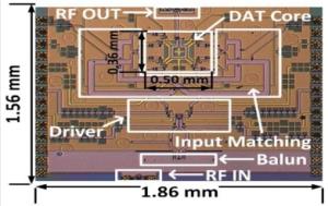
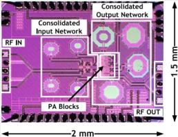
An F-Band Distributed Active Transformer PA
InP HBT 130 nm, 2022
This is a compact, low-loss distributed active transformer (DAT) for 8-to-1 power combining at 120 GHz. The proposed PA presents 11.5% power-added efficiency (PAE) and 8.6-dB gain at 22.1-dBm peak output power, and a 3-dB small-signal bandwidth from 100 to 140 GHz.
Designer(s): Linsheng Zhang, Vinay Iyer, Jay Sheth
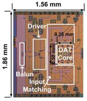
A Current-Mode Multiphase Digital Transmitter
CMOS 65 nm, 2022
This work demonstrates a current-mode multiphase digital transmitter with a single-footprint transformer-based asymmetric Doherty output network. The transmitter achieves more than 20-dBm output power (Pout) and more than 31% DE from 4.5 to 6.7 GHz. At 8-dB PBO, it achieves a DE of 23% and 24% at 6.5 and 7.0 GHz.
Designer(s): Jay Sheth, Linsheng Zhang, Xiaochuan Shen, Vinay Iyer
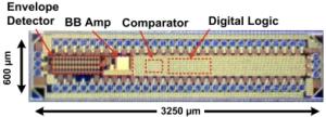
A Wake-Up Receiver with ADPLL
CMOS 65 nm, 2022
This work presents a 2.4GHz binary frequency-shift keying (BFSK) heterodyne WuRx with low-power All-Digital Phase Locked Loop (ADPLL) and sharp intermediate frequency (IF) filtering. It achieves -102dBm sensitivity with 2.2µA to 171µA power range at 16s to 100ms latency. It demonstrates a -27/-30dB continuous wave (CW) signal-to-interference ratio (SIR) at 3/5MHz offset from the carrier.
Designer(s): Linsheng Zhang, Divya Duvvuri, Anjana Dissanayake, Yaobin Zhang
An F-Band Stacked Power Amplifier
InP HBT 130 nm, 2022
This work presents a scalable modulation chain built using commercial equipment at 121 GHz and its demonstration using a 130-nm InP HBT PA. The PA has a 3-dB small signal gain BW from 90 to 135 GHz with a peak gain of 11.7 dB, a peak PAE of 18.3%, and a peak power of 15.3 dBm at 112.5 GHz.
Designer(s): Vinay Iyer, Linsheng Zhang
A DAT-Based Power Amplifier
InP HBT 130 nm, 2022
The DAT-based PA adopts a stacked transistor structure with compact geometry to minimize the imbalance caused by interwinding capacitance. In addition, capacitive tuning has been implemented at the output of the DAT to achieve direct matching to the unit PA. It achieves 22.1 dBm peak output power with 11.5 % PAE. The 3 dB bandwidth is across 100 GHz to 140 GHz.
Designer(s): Linsheng Zhang, Vinay Iyer, Jay Sheth
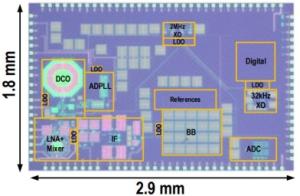
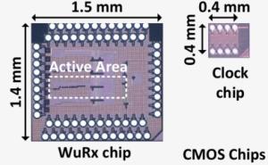
A Highly Integrated 2.4-GHz Wake-up Receiver
CMOS 65 nm, 2021
This is a highly integrated and scalable 2.4 GHz WuRX fabricated in a standard 65 nm CMOS process. The WuRX achieves a state-of-art performance of −91.5 dBm sensitivity with dc-power of 0.9–20.9 μW for 1 s–10 ms latency. The measured SIR demonstrates CW −47.5 dB and 16-QAM −19.5 dB/−32 dB for 3 dB/6 dB desensitization at 20 MHz offset.
Designer(s): Anjana Dissanayake, Henry Bishop
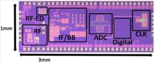
An Antenna-Coupled 4.9 GHz Wakeup Receiver
CMOS 65 nm, 2021
This is a highly-integrated, supply-robust, event-driven wakeup receiver achieving <-74 dBm sensitivity using a custom antenna at 4.9 GHz or <-68 dBm sensitivity when matched to a 50 Ω source at 5.3 GHz, both across a supply voltage range from 1.2 V to 1.5 V while consuming 244 nA dc current in 65 nm CMOS technology.
Designer(s): Divya Duvvuri, Xiaochuan Shen, Pouyan Bassirian, Henry Bishop, Xinjian Liu, Anjana Dissanayake, Yaobin Zhang
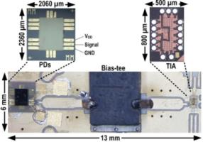
A SiGe BiCMOS Transimpedance Amplifier
SiGe 130 nm, 2021
This is a heterogeneously integrated low-noise microwave-balanced photoreceiver utilizing Si3N4 waveguide InP/InGaAs MUTC PDs based on the bonding of III-V material on silicon. The TIA achieves 74 dBΩ of transimpedance gain with a 1 dB peak, a bandwidth of 3 GHz, and a low equivalent input noise current density of 7.2 pA/√Hz when loaded with a CP D of 380 fF. The full photoreceiver achieves a high conversion gain of more than 2 kV/W up through 2 GHz, and a low NEP of 8 pW/√Hz up through 1.6 GHz. The photoreceiver optical CMRR is measured to be 36 dB.
Designer(s): Robert Costanzo, Xiaochuan Shen
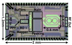
A Four-Way Nested Digital Doherty Power Amplifier
CMOS 65 nm, 2021
The PA uses a compact input and output matching network through the consolidation of components, and it achieves a peak drain efficiency (DE) of 48% and a system efficiency (SE) of 31% with 7.3 dBm of output power (Pout) and 14 dB of gain at 4.75 GHz. It also obtains a DE of 42% and 20% at 0- and 12.8-dB PBO, respectively, at 5.25 GHz, which corresponds to a 2.2× improvement over normalized class B PA. Finally, RF modulation measurements performed on the PA show that it achieves a DE of 34% and an RMS error vector magnitude (EVMrms) of −20.5 dB for a 1-MSym/s 16 QAM RF waveform at 5.25 GHz.
Designer(s): Jay Sheth
A Multichannel, MEMS-less Bit-level Duty Cycled Wakeup Receiver
CMOS 65 nm, 2020
This is a -99 dBm sensitivity, 260nW 434 MHz ISM band wakeup receiver (WuRX) in 65nm CMOS without MEMS filters, which is 18dB better sensitivity than any prior MEMS-less sub-µW design. Reconfigurable within-bit duty cycling of the tuned-RF front end trades power for latency between 260ms latency at 2.17µW and 2.6s latency at 260nW.
Designer(s): Anjana Dissanayake, Henry Bishop, Jesse Moody
A Transimpedance Amplifier With Input DC Photocurrent Compensation Loop
CMOS 55 nm, 2020
This TIA achieves a transimpedance gain of 69 dB across a 3-dB bandwidth of 10.7 GHz. Additionally, the TIA demonstrates low-noise performance with an equivalent input noise density of 15 pA/√ Hz in the passband. The dc compensation is capable of providing a fixed bias voltage for a PD while sourcing up to 2.4 mA or sinking up to 1 mA of photocurrent. The TIA, including active balun and dc current compensation, consumes 15.7 mW, while the output buffer consumes 90.7 mW. The total active area of the circuit is 0.07 mm^2, and 0.21 mm2 with pads.
Designer(s): Robert Costanzo
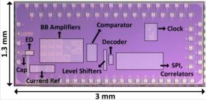
A S-Band Nanowatt-Level Wakeup Receiver With Envelope Detector-First Architecture
CMOS 65 nm, 2020
This 2.2 GHz S-band WuRx can operate in two modes that show a tradeoff between power consumption and RF sensitivity. In the low-power mode, the WuRx consumes 11.3 nW and achieves an RF sensitivity of −65 dBm. In the high-sensitivity mode, the WuRx consumes 28.2 nW and achieves a sensitivity of −68 dBm.
Designer(s): Pouyan Bassirian, Divya Duvvuri, Daniel Truesdell
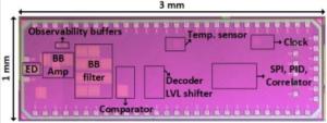
A Digitally Reconfigurable Bit-Level Duty-Cycled Wakeup and Data Receiver
CMOS 65 nm, 2020
This is a -108dBm sensitivity, 430MHz, 130nW-41µW, 6.25bps-4.2kbps, digitally tunable wake-up and data receiver. The WuRx is fully digitally programmable between 130nW-41µW dc power and 6.25bps-4.2kbps. Close-in SIR of -25dB and far-out SIR of -28dB allows for robust operation in a channel-crowded environment. Dynamic ranges of 11dB, 410X, 672X are achieved for sensitivity, power, and latency, which enable high post-fabricated tunability and firmware programmability after deployment in a network.
Designer(s): Anjana Dissanayake, Jesse Moody, Henry Bishop, Daniel Truesdell, Henry Muhlbauer
A Temperature-Robust Wakeup Receiver
CMOS 65 nm, 2020
This is a sub-100nW WuRx that is robust to temperature variation in the 0-to-70°C commercial range and operates at 9.6GHz X-band frequency. The WuRx achieves a sensitivity of -65dBm with <2dB degradation across the entire temperature range and consumes an average power of 27.6nW at 20°C.
Designer(s): Pouyan Bassirian, Divya Duvvuri, Daniel S. Truesdell
A Highly Reconfigurable Bit-Level Duty-Cycled TRF Receiver
CMOS 65 nm, 2019
This is a reconfigurable wake-up receiver, which obtains −106-dBm sensitivity with power consumption as low as 33 nW. Bit-level duty cycling provides 68-dB RF gain at sub-µW average power consumption, improving sensitivity over other sub-µW receivers.
Designer(s): Jesse Moody, Anjana Dissanayake, Henry Bishop, Divya Duvvuri, Daniel Truesdell
A Bit-Level Duty-Cycled Tuned RF Wake-up Receiver
CMOS 65nm, 2019
This is a 33 nW wake-up receiver with -106 dBm sensitivity at 428 MHz. Within-bit duty cycling allows RF gain at nano-watt DC power levels, providing 26 dB sensitivity improvement over prior art at iso-power. An RF MEMS filter and an automatic gain and offset control loop suppress noise and reject interference. The receiver can be digitally tuned across DC power, latency, and sensitivity to provide flexible functionality from indoor short-range to outdoor long-range applications.
Designer(s): Jesse Moody, Anjana Dissanayake, Henry Bishop, Ningxi Liu, Divya Duvvuri, Daniel Truesdell
Interference Robust Detector-First Near-Zero Power Wake-Up Receiver
CMOS 130 nm, 2019
This WuRx obtains −76 dBm at the 151.8-MHz multi-use radio service (MURS) band and −71 dBm at the 433-MHz Industrial, Scientific and Medical (ISM) band with a total dc power draw of just 7.6 nW from 1.0- and 0.6-V supplies.
Designer(s): Jesse Moody, Pouyan Bassirian, Abhishek Roy, Ningxi Liu
Nanowatt-Level Wakeup Receiver with MEMS Resonators
CMOS 130 nm, 2019
This WuRx achieves a sensitivity of −54 dBm with 7 nW of average dc power consumption without a digital correlator.
Designer(s): Pouyan Bassirian, Jesse Moody, Abhishek Roy
A Triode-mode Envelope Detector
CMOS 130 nm, 2019
This is an envelope detector topology based upon triode mode transistors operating as a chain of charge pumps. This detector offers superior tunability, performance, and robustness over the Dickson topology. This work utilizes a direct gate bias applied to complementary devices to form a single detector stage.
Designer(s): Jesse Moody
A Current Reuse Regulated Cascode CMOS Transimpedance Amplifier
CMOS 65 nm, 2018
This TIA is capable of achieving a 62-dB transimpedance across a −3-dB bandwidth of 11 GHz. The equivalent input current noise is measured to be 30 pA/√Hz, and the TIA core consumes 10 mW, with a 56 mW output buffer.
Designer(s): Robert Costanzo
A Balanced Photoreceiver
CMOS 130 nm, 2017
This TIA achieves a transimpedance gain of 39 dBΩ. The complete photoreceiver achieves a conversion gain of 41 V/W across a 10 GHz bandwidth with the TIA consuming 56 mW from a 2 V supply, and the PDs drawing 1.2 mA from +/-5 V supplies. High sensitivity is achieved due to a low noise equivalent power (NEP) of 86 pW/√Hz.
Designer(s): Robert Costanzo, Zhanyu Yang, Nicolas Raduazo