III-V APDs
III-V APDs
III-V digital alloy avalanche photodiodes (APDs) are highly suitable for LIDAR system and telecommunications applications due to their low excess noise and high gain-bandwidth product. The bandgap of these short-period superlattices can be easily tuned by altering the alloy composition or period thickness. Therefore, these APDs can be used in detecting a wide range of signals. We employ a Density Functional Theory (DFT) calibrated Environment-Dependent Tight Binding (EDTB) model to do a detailed study of the material physics of these alloys. We use quantum transport models like the Non-Equilibrium Green's Function (NEGF) formalism for understanding the effect of these material properties on carrier transport. Additionally, we are exploring the thermal properties of these APDs using DFT based simulations. Our goal is to develop a comprehensive modeling framework for these photodetectors that can be used to investigate the material properties, carrier transport, and circuit-level performance.
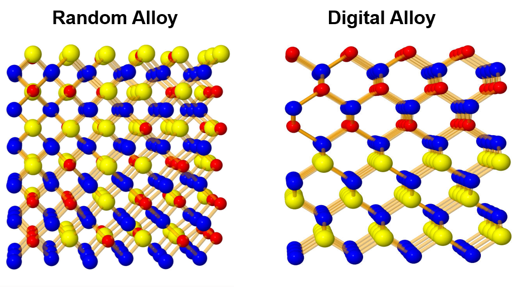
In traditional III-V alloys, called random alloys, constituent atoms are distributed in a random manner. III-V digital alloys are short-period superlattices where the binary components are stacked alternately in a periodic manner. These alloys are grown using the state-of-the-art Molecular Beam Epitaxy (MBE) technique. These structures have unique and interesting properties that we believe enhance the performance of the digital alloy APDs.
We have calculated the bandstructure of various digital alloys using an Environment-Dependent Tight Binding Model. This model incorporates the interaction of an atom with its neighboring atoms and thus can accurately capture the impact of various effects like strain. Afterward, using a band unfolding technique we create simple pictures of the complicated band structure of the large supercells. These pictures show the presence of small bandgaps, called 'minigaps', and enhanced hole mass in some of these alloys. These properties directly correlate with the low excess noise performance of these alloys.
Furthermore, we are developing detailed carrier transport models so as to understand the role of these minigaps on electron and hole movements in the device. Currently, our group is developing a detailed quantum transport model using the Non-Equilibrium Green's Function (NEGF) formalism to study both coherent and incoherent transport processes in the digital alloy APDs.
In addition to their unique electron transport characteristics, these alloys also have interesting thermal properties that impact the temperature-dependent APD performance characteristics and are not well understood. Our work in this area involves using phonon dispersions and semi-analytical models to link the thermal properties of these superlattices to the real device performance.
Presently, there is also a growing interest in integrating photodetectors with CMOS technology for application in the fields of Internet of Things (IoT) and 5G communication. Large semiconductor companies like Intel are developing photonic integrated circuits for such applications. Moving towards that goal our group is developing a multiscale compact model of these APDs for use in circuit simulations. One of our long term objective in this area is to design new photonic integrated circuits that utilizes these III-V digital alloy APDs.