Graphene Electronics
2 April 2012
Transport in graphene:
The search for a replacement to Silicon based digital electronics resurrected interest in graphene, a 2-dimensional carbon allotrope. Various 1D derivatives of graphene such as carbon nanotubes and nanoribbons have also become topics of extensive research in the past half a decade. We are particularly interested in how the rich chemistry of graphene and its various derivatives influence fundamental electronic properties, device performance and basic circuit-level issues. We implore both analytical and numerical methods to understand various aspects of graphene’s fundamental electronic structure, device and circuit level properties. In terms of fundamental electronic properties we posed several questions to answer:
- The role of edge chemistry and roughness on bandgap or device off-state
- What is common thread that links graphene and its derivatives to basic aromatic hydrocarbons and the role it plays on bandstructure
- Does opening a bandgap in graphene’s low-energy linear bandstructure degrade intrinsic mobility even in the absence of externally influenced scattering processes?
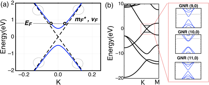
- Opening bandgaps destroy low energy band linearity increasing effective mass. and decreasing mobility. Beyond fundamental electronic properties and into devices we explored:
- The device performance enhancements of an all graphene patterned field effect transistor.
- How does edge roughness in nanoribbons influences device performance variability?
- The development of a physics compact level models for graphene field effect transistors to evaluate circuit level performance using Cadence.
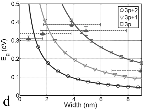
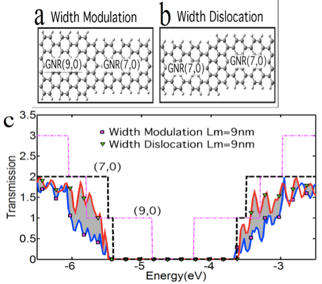
Edge roughness in graphene nanoribbons filters the smaller bandgap and promotes the largest bandgap. An explanation for the lack of 3 chiralities in experiments that are predicted theoretically.
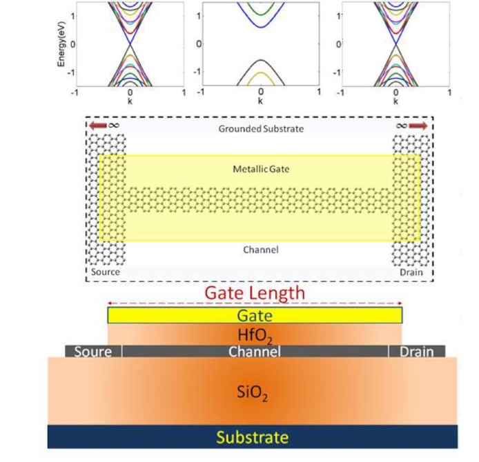
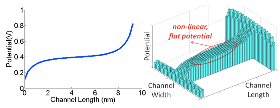
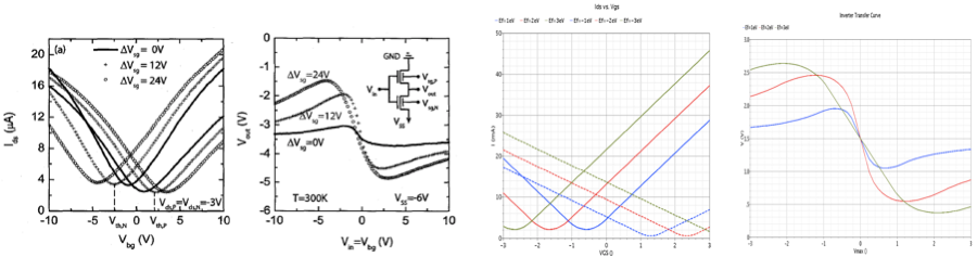
An all graphene patterned field effect transistor benefits from 2D electrostatics from the source and drain that ensure better gate control shown by the flat potential along the length of the channel. Source-drain graphene contacts also ensure Ohmic contacts which removes Fermi level pinning typical with metal contacts.
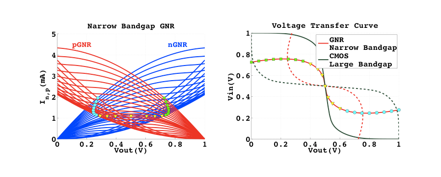
Lack of a bandgap in large area graphene and immediate onset of band-to-band tunneling degrades inverter voltage transfer curves as tunneling current inhibits complete pull-up and pull-down.
Electron optics, metamaterials and Klein tunneling:
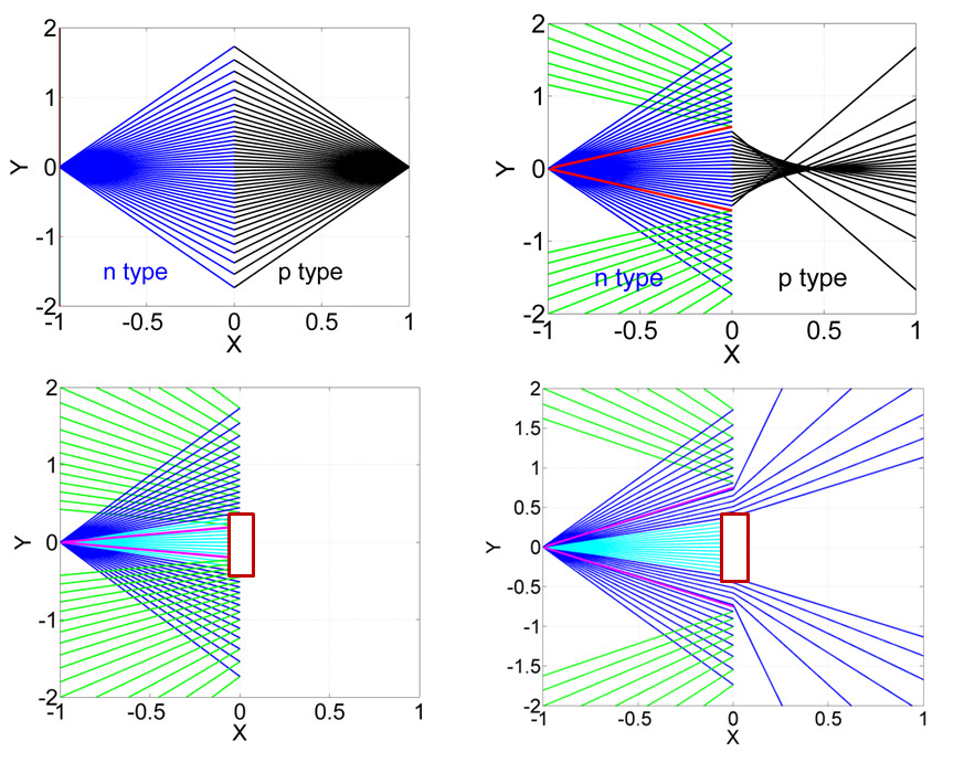
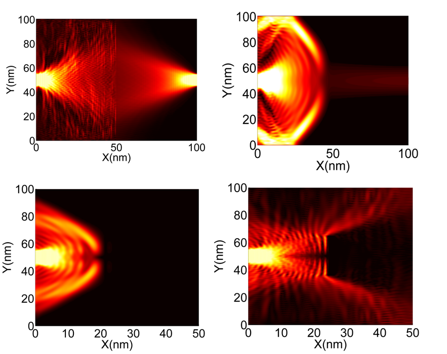
Graphene pn junction offers the platoform to draw analogy between optics and electronics. As a result, we can design many electrical devices using optical principles such as Ray Optics. Fig. 1(a) shows the electron trajectories for an electrostatically doped graphene pn junction, electrons bend at the interface, in order to conserve group velocity and the transverse momentum. The analogous Snell’s law can be formulated from this conservation of momentum. This produces an electron lens similar to Veselago lens in optics. Fig. 1(b) shows the case when electrons are going from higher doped region to a lower doped region. Electrons outside the critical angle reflect back. Fig. 1(c),(d) shows a novel device concept by using a tunnel barrier to eliminate energetic electrons to suppress Klein tunneling. It is theoretically predicted that this will induce a voltage dependent transmission gap, which can also be collapsed with gate voltage. Fig. 2 shows the NEGF simulation of the predicted results.