Beyond CMOS switches
Electronic Ratchet: non-equilibrium switching:
Electronic ratchet is novel non-equilibrium that is capable of driving current in the absence of an applied drain bias, by using a time varying, spatially asymmetric potential. The ratchet generates net current flow from the drift-diffusion process of charge carrier, acting as a voltage-controlled current source. The static dissipation associated with drain bias and dynamic dissipation connected with charging/discharging of load capacitors are reduced.
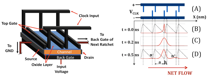
(LEFT) Physical Structure of an electronic ratchet, showing the interdigitated top gate creates the asymmetric time varying potential to drive the current through the channel. (A): Interdigitated electrodes between two conductor planes creating the desired asymmetric local potential profile in the channel. (B): Initial carrier distribution when potential is on. (C): Distributed carriers when potential is off. (D): electron distribution when potential is again turned back on at the heated state.
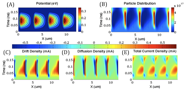
(A) shows how the asymmetric ratchet potential changes with time and space. (B) shows how the particles are evenly distributed (localized) in bins when the potential is raised and how they move to the right with the oscillating top gate (the light blue lines between localized bins shows the pathway of particles moving right). Subfigures below show the total, drift, and diffusion current densities. One can see that drift current opposes the diffusion current at all the times, but their magnitudes are different thus resulting in a net flow to the right. As discussed in the previous sections, the second phase of the two-part drift current shown in yellow moves the particles to right, then the diffusion current spreads the particles evenly right and left.
Nano-Electro-Mechnical Field Effect Transistor (NemFET): Miscroscopic modeling:
NemFETs are one of the device alternatives to the conventional CMOS with zero leakage and infinite sub-threshold slope that can be fabricated on variety of substrates including, silicon, glass, and plastic. Our model captures and explains the reason why a Hysteresis occurs in these devices with the use of potential profiles, Fokker-Plank, and Landauers theorem.

This model device shown above starts in the OFF configuration where there is no physical connection between source (S) and drain (D). With positive Gate (G) bias, the rod gets pulled down as in the figure and making contact thus turning the device on ON. There is a voltage difference when the lever pull-in and pull-out due to the surface charges and bonds, causing the hysteresis at the IV level.
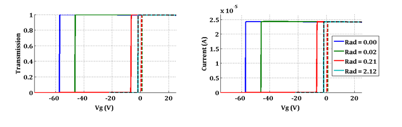
Also there is a direct dependence of scan-rate (angle of measurement) and the hysteresis. If our rod is fluctuating at higher angles (slower scan rate), the Hysteresis disappears, both pull-in and pull-out converges into one transition (show in Black and Cyan).