Body Sensor Networks
Battery-less Internet of Things (IoT) System-on-Chip (SoC)
A 1 trillion node internet of things (IoT) will require sensing platforms that support numerous applications using power harvesting to avoid the cost and scalability challenge of battery replacement in such large numbers. Our previous SoCs achieve good integration and energy harvesting, but they limit supported applications, need higher end-to-end harvesting efficiency, and require duty-cycling for RF communication. In this project, we demonstrates a highly integrated, flexible SoC platform that supports multiple sensing modalities, extracts information from data flexibly across applications, harvests and delivers power efficiently, and communicates wirelessly.

Chip Overview
The SoC has two main sensing interfaces: a 4-channel (2µW/channel) analog front-end (AFE) with an 8-bit analog-to-digital converter (ADC) and SPI with variable voltage output pads (0.4-to-3.3V) for commercial sensor compatibility. The Opencores MSP430 (OMSP) processor and a suite of accelerators can execute numerous biomedical and environmental signal processing algorithms (e.g. filtering, peak detection, histograms) combining ASIC energy efficiency and flexibility. A Lightweight Control Unit (LCU) can manage chip data and node control while the OMSP is off, and uses a custom instruction set architecture (ISA) and interrupt-driven programs to reduce the program size. The chip’s flexible clocking unit, containing a programmable all digital phase locked loop (ADPLL) and system clock configurability, can drive the system clock from a low power crystal. The digital blocks run in the sub-threshold regime on a 0.5V supply delivered by the PMU. The SoC uses an asymmetric transceiver architecture for data transmission and reception with 1) An ultra wideband (UWB) transmitter and 2) A narrowband wakeup receiver respectively.

Energy Harvesting and Power Management
The integrated energy-harvesting and power management unit (EH-PMU) couples a boost converter and a SIMO DC-DC regulator for power delivery to the SoC. The EH-PMU leverages two off-chip high-Q inductors (for the boost converter and the regulator) and an off-chip storage capacitor (or a super-capacitor) for storing harvested energy. The boost converter can harvest from a photovoltaic (PV) solar cell (e.g., with open circuit voltage of 1.7V) or from a TEG (e.g. with input voltage VIN as low as 10mV) and charge the storage capacitor up to VCAP=1.4V. An integrated maximum power point tracking (MPPT) circuit tunes the input impedance of the boost converter to extract maximum energy from the ambient source (either TEG or PV). The SIMO utilizes a buck-boost architecture to provide regulated outputs of 1.2V and 0.5V from a minimum input voltage (VCAP) of 0.7V provides a peak end-end efficiency of 75% at 1.2V output delivering a 100uA load current. Both the SIMO and the boost converter operate in Discontinuous Conduction Mode (DCM) to minimize conduction losses. The control scheme in both the boost converter and the SIMO consists of a peak inductor current control scheme that ensures constant peak current in the inductor with pulse-frequency-modulation (PFM) control to reduce conduction loss and a zero crossing detector to minimize conduction losses across the diode. The PMU also includes a cold-start circuit with a startup voltage of 220mV.

Digital Engine
The chip uses two 16-bit independent buses, each controlled by a separate controller. Bus 1 is controlled by either the OMSP or LCU, while Bus 2 is controlled by a two-channel DMA. Both buses have access to all the peripherals within the SoC. At startup, the LCU is the main controller on the chip and can configure the OMSP as the main controller of Bus 1 or as a bus peripheral that is used only for ALU or background operations. The chip has a 4kB data memory and three 2kB memories: the LCU instruction memory, the OMSP instruction memory, and the radio transmitter buffer.
The SoC also has a suite of programmable hardware accelerators to support energy efficient digital operation for common functions including an FIR filter, a CORDIC block, an FFT/IFFT, two timer modules, a multiplier, a histogram, and a heart rate (R-R) / atrial fibrillation (AFIB) detection block.

The SoC also contains a digital power management unit (DPM) that monitors the harvested energy by measuring the voltage on the storage capacitor and controls the different peripherals to ensure that the chip does not lose power when energy-harvesting conditions are poor. The DPM has three voltage thresholds that set the operating mode of the chip (green, yellow, or red). In green mode, the storage capacitor is nearly full, and the chip can perform any functionality. In yellow mode, the storage capacitor is being drained, and the chip must use its energy resources more efficiently. In red mode, the chip is approaching loss of power, and only essential operations must be performed.
Asymmetric Ratio
The UWB transmitter (Tx) uses OOK modulation with a data rate of 187.5kbps, chosen to match the data rate of the 802.15.6 WBAN standard. The center frequency is 3.994GHz with a 500MHz bandwidth. It consists of a pulse-width generation circuit to create a short pulse, which is then used to enable/disable a ring oscillator, creating the UWB pulses of period 2ns. A Class AB power amplifier buffers the signal onto the antenna. A finite state machine (Tx FSM) controls the data transfer and contains a 2kB sub-threshold memory buffer that stores the raw data to be transmitted.
To build a low power wakeup receiver (WRX) a narrowband RF link is chosen. A rectifier is used to replace the power hungry LNA and a bank of 31-bit CDMA codes is used for synchronization. From the antenna and band-select filter, the RF signal passes through an off-chip 2-element passive matching network that boosts the signal in 5dB before going into the rectifier. A 30-stage rectifier working in the sub-threshold region is used to directly down convert the RF signal to baseband. To synchronize the transmitted code and issue a wakeup, a bank of four correlators continuously correlates the 4x-oversampled comparator bit-stream with a programmable, 31-bit CDMA code. The baseband processor is synthesized in sub-threshold in order to save power.

Demo
To demonstrate maximum power point tracking (MPPT) and system startup, we used a commercial solar cell. It was observed from measurements that the boost converter enabled the MPPT loop to tune the input impedance of the boost converter so that the solar cell is loaded to operate at its maximum power point. After the harvested energy is stored on the storage capacitor, the necessary power can be provided to the SoC for continuous operation. In addition the chip was tested end-to-end for motion capture with an accelerometer while powered from indoor solar by the PMU. Acceleration data is fed to the FIR filter for DC filtering and the output is transmitted over the radio to an aggregator.


Faculty
Ben Calhoun (UVA), David Wentzloff (University of Michigan)
Research Scientist: Dilip Vasudevan (UVA)
Students: Abhishek Roy (UVA), Farah B. Yahya (UVA), Xing Chen (UMich), Christopher Lukas (UVA), Divya Akella (UVA).
UVA Graduated Students: Alicia Klinefelter (Intel), Patricia Gonzalez (UVA), Jim Boley (Psikick), Kyle Criag (Psikick), Yousef Shahsheer (Psikick), Aatmesh Shrivastava (Psikick)
UMich Graduated Students: Muhammad Faisal, Seunghyun Oh, Nathan E. Roberts (Psikick)
Tri-Modal Photoplethysmography Sensor Interface
This work presents a tri-modal self-adaptive photoplethysmography (PPG) sensor interface IC for concurrently monitoring heart rate, SpO 2 , and pulse transit time, which is a critical intermediate parameter to derive blood pressure. By implementing a highly-reconfigurable analog frontend (AFE) architecture, flexible signal chain timing control, and flexible dual-LED drivers, this sensor interface provides wide operating space to support various PPG-sensing use cases. A heart-beat-locked-loop (HBLL) scheme is further extended to achieve time-multiplexed dual-input pulse transit time extraction based on two PPG sensors placed at fingertip and chest. A selfadaptive calibration scheme is proposed to automatically match the chip's operating point with the current use case, guaranteeing a sufficient signal-to-noise ratio for the user while consuming minimum system power. This paper proposes a DC offset cancellation (DCOC) approach comprised by a logarithmic transimpedance amplifier and an 8-bit SAR ADC, achieving a measured 38 nA residue error and 8.84 μA maximum input current. Fabricated in a 65nm CMOS process, the proposed trimodal PPG sensor interface consumes 2.3 - 5.7 μW AFE power and 1.52 mm2 die area with 102dB (SpO 2 mode), 110 – 116 dB (HR & PTT mode) dynamic range. A SpO 2 test case and a HR & PTT test case are both demonstrated in the paper, achieving 18.9 μW and 43.7 μW system power, respectively.
A Battery-less 19uW MICS/ISM-Band Energy Harvesting Body Area Sensor Node SoC

Body Sensor Nodes
Body area sensor networks (BASNs) are rapidly becoming important tools in today's health care. However, the growing trend for portable health care is constrained by flexible on-node processing and very long device lifetimes. Increased life time of these devices will result in reduced cost to consumer and less invasive procedures to replace batteries/nodes. In this project, we utilize the state-of-the-art in low power RF transmitters, low voltage boost circuits, subthreshold processing, biosignal front-ends, dynamic power management, and energy harvesting to realize an integrated reconfigurable wireless body area sensor network (BASN) SoC capable of autonomous power management for BATTERY-FREE operation.
Chip Overview
Our chip has many stringent constraints in order to meet our requirements for a battery-less and flexible BASN platform, some of which include: • Ultra low total chip power for sustainable operation using TEG • Voltage regulation to convert ultra low voltage input (10’s mV) to usable voltage, and to supply different voltage domains across the chip • Various analog bio-signal acquisition, amplification, and digitization • Ultra low power, re-programmable digital signal processing for energy efficient adaption of various algorithms • Low power transmission and flexible data rates • Total chip power management for efficient power-steering to the essential circuit components Here is the chip architecture solution to our many challenges:

Architecture Explained:
Energy Harvesting / Supply Regulation (top left): An energy harvesting/supply regulation section boosts an input as low as 30mV up to a regulated 1.35V supply. In the end we use a hybrid energy harvesting subsystem, allowing operation from RF and/or thermoelectric power sources. Small body-worn TEGs typically provide very low output voltages (<100mV), but we employ an ultra-low voltage boost converter capable of boosting voltages as low as 30mV. However, the control circuit to our boost converter will not work until ~600 mV is supplied to it. So solve this problem, a one-time kick-start is provided wirelessly through an RF rectifier front-end with incident power as low as -10dBm. The node will then continue to run indefinitely from the TEG.
Power Management / Signal Processing (top right): A subthreshold digital section performs data processing, mode control, and power management (including power/clock gating of blocks and dynamic voltage scaling (DVS)) based on the available energy on the storage capacitor that stores the energy harvested from the TEG. The digital section includes a custom digital power management (DPM) processor, general purpose microprocessor (MCU), programmable FIR, 1.5kB instruction SRAM / ROM, 4kB data SRAM, and dedicated accelerators for ECG heart rate (R-R) extraction, atrial fibrillation (AFib) detection, and EMG band energy calculation. This section is truly the 'heart' of the BASN chip. Not only is the DPM available to manage the whole chip, the flexibility of this digital processing subsystem makes it so processing through the MCU, fully custom processing with accelerators, or a mixed approach is readily available based on application needs. The digital subsystem is capable of processing the bio-signals at an ultra low energy consumption in the sub-nanowatt range.
Analog Front End (bottom left): An analog front-end (AFE) with programmable gain and a successive-approximation (SAR) ADC amplifies and digitizes signals as low as a few μVs. The chip has four independently selectable biosignal input channels. Our amplifiers provide digitally-programmable gain (40-78dB) from DC to 320 Hz at 3μW/channel, compatible across many different bio-signal types.
Frequency-Multiplying Transmitter (bottom right): We utilize a transmitter architecture that consumes 160µW when transmitting at its maximum data rate of 200 kbps. Though this greatly relieves the transmitter (TX) as being the total chip power hog, it is still not efficient enough to be transmitting at 100% duty cycle and leave enough energy on the storage capacitance for a sustainable battery-less chip. However, the data extraction from the digital signal processing portion, for example running the R-R extraction algorithm reduces the duty cycle and average transmitter power consumption to 0.013% and 190nW respectively. The packetizer contains a programmable packet header and CRC (cyclic redundancy check) to allow compatibility with commercial receivers.
Demos

An ECG experiment was performed on a healthy human subject. First, the chip was set to ECG raw data mode (consuming 397μW). Data was transmitted to a TI CC1101 receiver. The reconstructed ECG closely matched the actual ECG (top). Next, the chip used the on-chip R-R interval extractor to transmit measured heartrate every 5s operating from a 30mV supply voltage (bottom). Every 5s, sufficient available energy is checked, in which case the crystal oscillator is enabled for 20ms before the TX transmission (650μs including turn-on time and transmitting 24b). The heart rate extractor algorithm measures the R-R interval with a time resolution of (1/128)s. The total chip power is 19μW.
Faculty
Ben Calhoun (UVA), Brian Otis (University of Washington)
Students: Yanqing Zhang (UVA), Yousef Shahsheer (UVA), Jim Boley (UVA), Alicia Klinefelter (UVA), Aatmesh Shrivastava (UVA) Helen Zhang (UW), Jason Silver(UW), Manohar Nagaraju (UW), Jagdish Pandey (UW)
Electrocardiogram System-on-Chip for Remote Health Monitoring
This project centers on the development of a custom system-on-chip (SoC)for electrocardiogram (ECG) acquisition and analysis. ECG data is important for medical diagnosis of general health and of many specific conditions, including a variety of cardiac arrhythmias. Existing methods of capturing ECG outside of the clinical setting, such as Holter monitors or event monitors, either have limited lifetimes or non continuous acquisition. This project seeks to develop custom hardware to dramatically extend the lifetime of ECG acquisition circuits by fabricating a custom SoC.
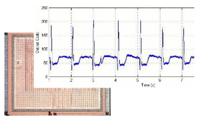
To determine the features required on the chip, we first developed a discrete prototype of the system. The prototype used commercial off the shelf (COTS) hardware in a custom system that acquired ECG data and wirelessly communicated it to a handheld. The first prototype of the custom IC integrated the analog front end and the digital processing onto a system on chip. The 130nm CMOS SoC uses low voltage design for energy efficient operation. Our chip gallery gives more more details on the chip. The analog front end comprises an instrumentation amplifier and an analog to digital converter. These analog components are biased in sub-threshold to reduce current consumption. The digital processor is a custom microcontroller based on the PIC architecture. The microcontroller operates in the sub-threshold region. Its minimum energy voltage occurs at 280mV, where it was measured to consume just 1.5pJ per instruction. The SoC can acquire ECG data and execute a heart rate extraction algorithm while consuming only 2.6uW.
Faculty
Ben Calhoun, Travis Blalock
Students: Steve Jocke, Jonathan Bolus, Stuart Wooters
A COTS Based Low Power Wireless ECG Sensor

In this project, a low power wireless ECG sensor is implemented using commercial off the shelf (COTS) components. The resulting system can acquire and process ECG data and send it wirelessly to a basestation such as a handheld device. The picture shows the ECG sensor in operation, with the PDA plotting the real time ECG signal.
The COTS ECG sensor provides a flexible platform for exploring different low power design techniques and measuring data to analyze these methods. Especially of interest is wireless communication, which consumes the most power of any single component. We have explored the impact on the system of using different radios.

We have also developed a complete back end that couples to this ECG sensor. The back end software can run on a mobile device or a PC. It aggregates, stores, processes, and displays data transmitted by the ECG sensor, and it can support multiple concurrent users.
Faculty:
Travis Blalock, Ben Calhoun, Alf Weaver (CS)
Students: Jonathan Bolus, Andrew Jurik
Assist Center

The Advanced Self-Powered Systems of Integrated Sensors and Technologies (ASSIST) Center is a new NSF Nanosystems Engineering Research Center (NERC) that will develop and employ nano-enabled energy harvesting, energy storage, nanodevices and sensors to create innovative battery-free, body-powered, and wearable health monitoring systems. The four partner schools in the center are NC State, UVA, Penn State, and Florida International University. Our group is leading the integration of the center technologies into a complete electrical system for wearable health and personal environmental monitoring.
The ASSIST center envisions a paradigm shift in health informatics enabled by wearable nanotechnologies that monitor individual health parameters and environmental exposures. Long-term sensing will enable patients, doctors, and scientists to make direct correlations between health and environmental toxins leading to chronic disease prediction, management and treatment. ASSIST advances will accelerate environmental health research and clinical trials as well as inform environmental policy.
The integrated sensor nodes that we are developing for ASSIST will include advanced energy harvesting and energy storage materials, novel devices, and nano sensors developed in the center. A BSN platform SoC, inspired by our prior work in this area, will provide data acquisition, power delivery and management, computation, data storage, and communication for the system. ASSIST will deploy its technology in a wearable form factor like a wristband or patch and then evaluate it in testbeds for both personal wellness and personal environmental monitoring.

Faculty
Ben Calhoun (UVA), Dave Wentzloff (U Michigan)
Students: Farah Yahya (UVA), Chris Lukas (UVA), Abhishek Roy (UVA), Divya Akella (UVA) Xing Chen (UM)