FEI Quanta 650 Scanning Electron Microscope
About
Location: Wilsdorf B003
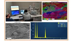
The Schottky Field Emission SEM microscope is capable of imaging and microanalysis on all specimens, with or without preparation. Characterization of both traditional samples from metals, fractures and polished sections, to non-conductive soft materials. Attachments for elemental analysis with Energy-Dispersive X-ray Spectroscopy (EDS) and for grain orientation mapping with an Electron Back-Scatter Detector (EBSD).
SEM Technique Summary:
- SEM and Compositional Analysis of Metals, Glasses, Semiconductors, Ceramics, Polymers, Geologic Materials, Catalysts, Pharmaceuticals, etc.
- High vacuum imaging: <0.25 mTorr
- Low-vacuum imaging: 0.25 mTorr to 1.5 Torr
- Environmental SEM (ESEM): 1.5 Torr to 6 Torr
- Secondary Electron (SE) imaging for topographic contrast
- Back-Scattered Electron (BSE) imaging for chemical contrast
- Scanning Transmission Electron Microscopy (STEM) option for imaging of thin samples
- Quantitative Elemental Analysis and Mapping of Materials with EDS
- EDS Elemental Sensitivity:> 0.1 wt.% (weight percentage) for Z > 5 (B)
- Mapping of grain orientations, texture and phase analysis with the EBSD system
- Montage imaging of large samples
- Sample size up to 4 x 15 x 15 cm³ ( H x W x D)
Quanta 650 Features:
- High resolution Schottky field emission
- SEM column optimized for high brightness/high current
- High vacuum imaging with beam deceleration up to 4 kV: Landing energy: 200 V to 30 kV
- Imaging resolution in high vacuum mode at 30 kV: 0.8 nm (STEM), 1.0 nm (SE), 2.5 nm (BSE)
- Wet STEM stage for viewing TEM samples/ ESEM samples
- 3 nm SE resolution at 1 kV in high vacuum mode and at 3 kV in low-vacuum mode
- Imaging resolution in low vacuum mode at 30 kV: 1.4 nm (SE), 2.5 nm (BSE)
- Oxford Silicon drift detector (SDD) with 150 mm window for EDS
- Oxford EBSD system for grain orientation mapping
- Oxford Aztec software for EDS and EBSD
- Maximum horizontal field width: 5 mm at analytical working distance of 10 mm; 18.8 mm at 65 mm WD
- Probe current: ≤ 200 nA, continuously adjustable
- Magnification: 6 to 1000000x
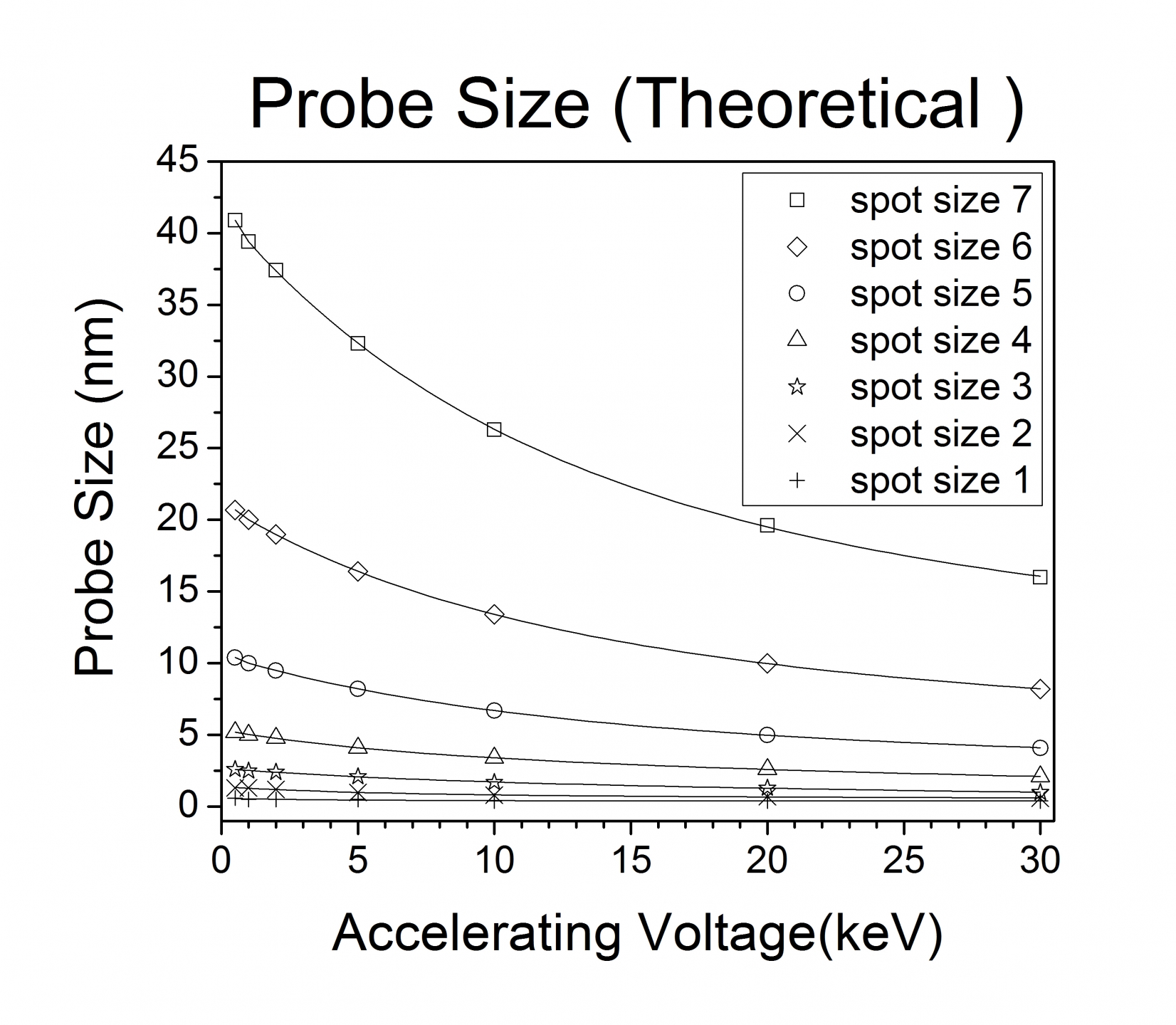
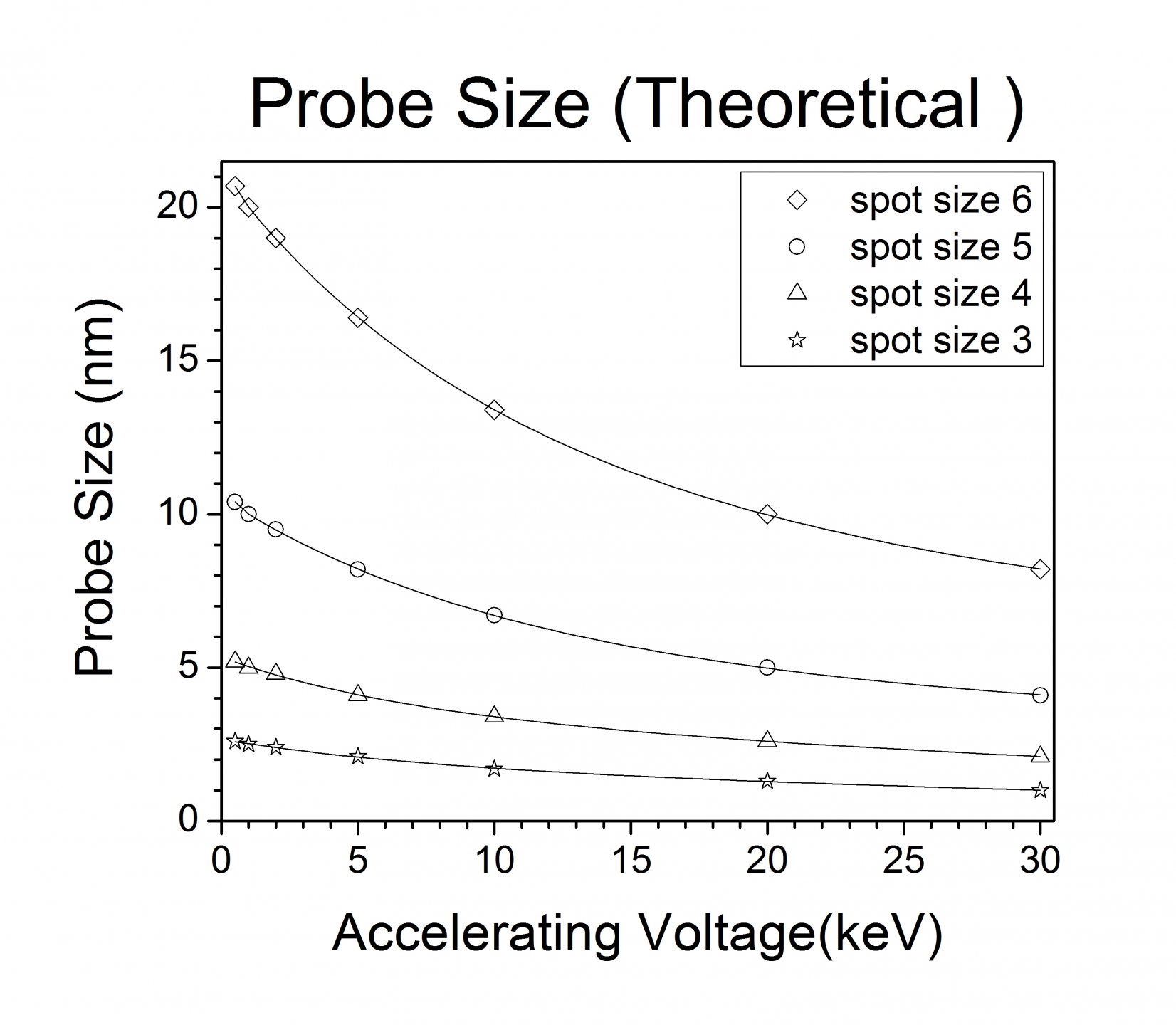
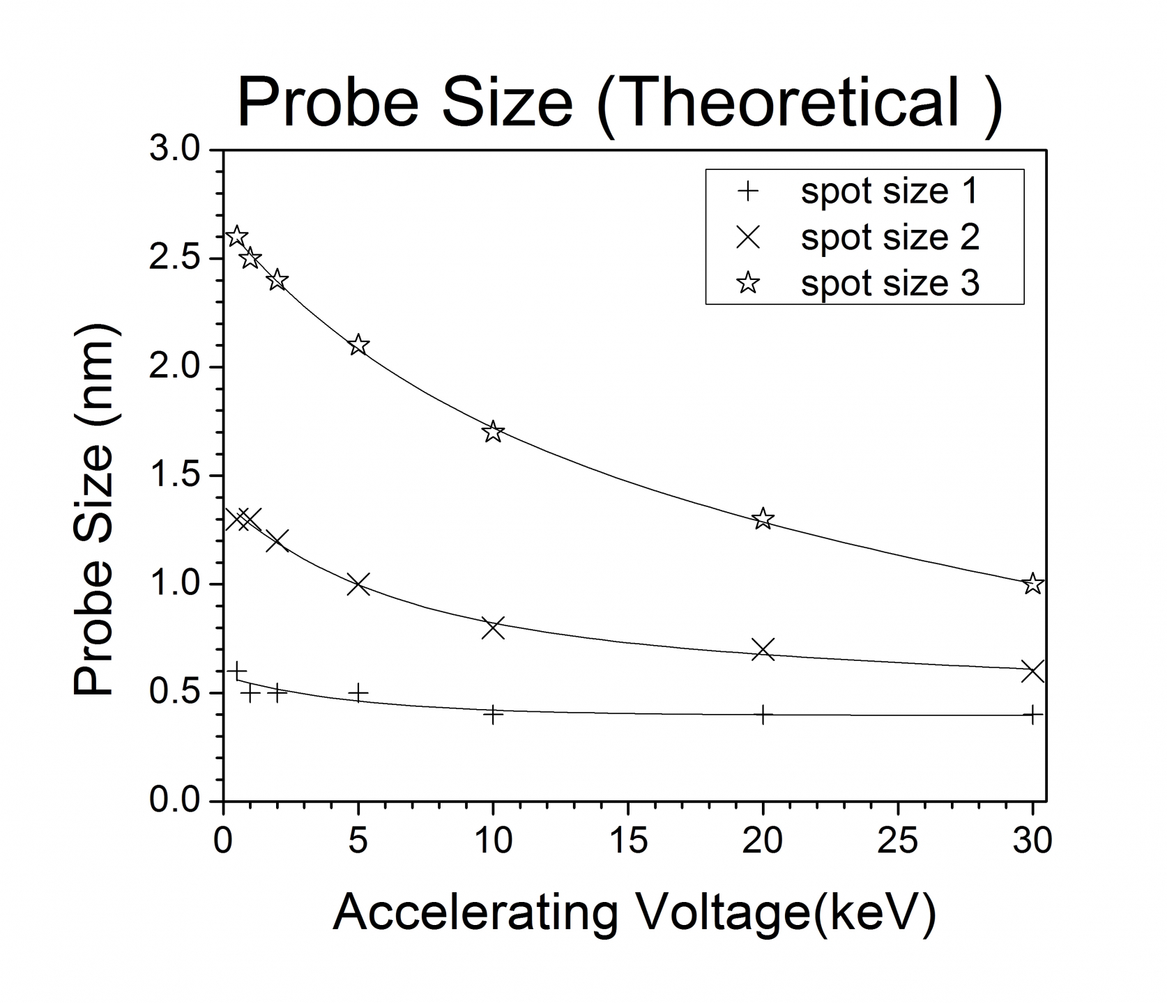
Electron Beam Size Calibration Graphs:
EDS available with Spot Size 5, 6, and 7
Rates
UVA RATES:
Quanta 650 FE-SEM Instrument Usage: $50/hr (8AM - 5PM) & $39/hr (after 5PM)
Quanta 650 FE-SEM Operator Costs: $60/hr
EDUCATIONAL, GOVERNMENT & NON-PROFIT INSTITUTIONS RATES:
Quanta 650 FE-SEM Instrument Usage (Operator Costs Included): $130/hr
INDUSTRIAL PARTNER RATES:
Quanta 650 FE-SEM Instrument Usage (Operator Costs Included): $325/hr
Contact Us
Richard White
Facility Manager, SEM, TEM, FIB, Optical, Metallography
Joe Thompson
NMCF & VTRC , Laboratory Specialist, Metallography, Optical, SEM, Raman/AFM, Profilometer