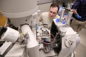
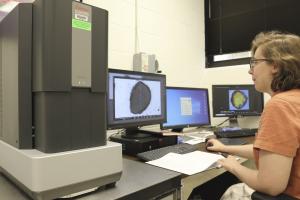
Electron Microscopy
Electron microscopes come in two broad varieties: transmission electron microscopes (TEMs) and scanning electron microscopes (SEMs). Both instruments provide high-resolution imaging and 1-D and 2-D compositional information.
SEMs provide surface images and information about topography by scanning the sample with a focused beam of electrons and monitoring the commensurate secondary electron signal. High-contrast images using backscattered primary electrons (EBSD) can provide general information about atomic mass. An energy dispersive X-ray detector (EDS) on the SEM gives elemental composition with excellent spatial resolution (~10 nm) and an information depth of ~ 5 microns. Sample composition can be found at a point, series of points, across a line or over an area.
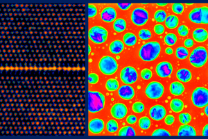
TEMs provide nanoscale or atomic-scale images of thin sections of a material, where high-energy electrons pass through the sample to form the image or provide crystal structure information, including phase. The narrow beam of electrons can also provide elemental information via EDS as a function of position (maps). The addition of an electron spectrometer on our TEM allows electron energy loss spectroscopy (EELS) for measurement of atomic composition (particularly light elements), chemical bonding, and valence and conduction band electronic properties.
NMCF Electron Microscopes
-
Titan High-Resolution Scanning TEM
Atomic-scale imaging and characterization of materials by high-resolution transmission electron microscopy (TEM), scanning TEM (STEM) and integrated energy-dispersive X-ray spectroscopic (EDS) analysis. Nondestructive composition (Z > 5) and bright-field/dark-field techniques. Cryo- and heating stage options.
-
Themis High-Resolution Scanning TEM
Materials imaging with atomic-scale resolution in both transmission electron microscopy (TEM) and probe-corrected scanning TEM (STEM) modes. Energy-dispersive X-ray spectroscopic mapping (EDS) and electron energy-loss spectroscopy (EELS). Bright-field, dark-field, high-angle annular dark-field (HAADF), and differential-phase contrast detectors.
-
Helios Dual-Beam FIB / SEM / STEM
Focused ion mill for TEM sample preparation & scanning electron microscopy (SEM). E-beam and I-beam deposition. Quantitative elemental mapping by energy-dispersive X-ray spectroscopy (EDS); crystallographic analysis by electron backscatter diffraction (EBSD); Scanning TEM, secondary (SEI) and backscattered electron imaging (BEI).
-
FEI Quanta 650 Field Emission SEM
Nano-scale scanning electron microscopy (SEM) with field-emission source for high-resolution imaging and microanalysis of sections of all types. Compositional microanalysis with energy-dispersive X-ray spectroscopy (EDS); microstructural-crystallographic characterization and strain by electron backscatter diffraction (EBSD).
-
Thermo Phenom XLG2 SEM
Nanoscale scanning microcopy (SEM/ESEM) with with backscattered (BEI) and secondary (SEI) electron imaging, as well as energy-dispersive X-ray spectroscopy (EDS) for enhanced materials characterization without time-consuming sample preparation.
Contact Us

Helge Heinrich
Dr. Helge Heinrich joined the NMCF as the Principal Scientist for High-resolution Transmission Electron Microscopy, with expertise in focused ion beam sample preparation and cross sectional electron microscopy (FIB-SEM) from the University of Central Florida.

Joe Thompson
Joe Thompson joined the NMCF as a Laboratory Specialist, also providing analysis for the Virginia Department of Transportation (VDOT). He specializes in Raman Spectroscopy, Atomic Force Microscopy, and Optical and Electron Microscopies.