Helios UC G4 Dual Beam FIB-SEM
About
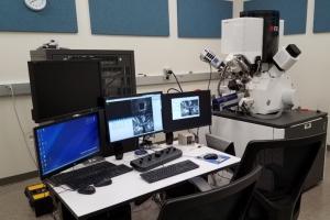
Location: Wilsdorf B001
The dual-beam Helios UC G4 from Thermo Fisher Scientific is used for site-specific modifications of samples using the Ga ion-beam unit. Ion milling can be combined with carbon and platinum deposition. Sample cross sections and thin slices for Transmission Electron Microscopy (TEM) are prepared with this Focused Ion Beam (FIB) system. Scanning Electron Microscopy (SEM) can be combined ion milling to obtain 3-dimensional data. The Helios offers Energy Dispersive X-ray Spectroscopy (EDS) for compositional analysis and Electron Back-Scatter Diffraction (EBSD) for texture measurements.
FIB-SEM Technique Summary:
- SEM and Compositional Analysis of Metals, Glasses, Semiconductors, Ceramics, Polymers, Geologic Materials, etc.
- High vacuum imaging and sample processing: <0.07 mTorr
- Quantitative Elemental Analysis and Mapping of Materials with EDS
- EDS Elemental Sensitivity:> 0.1 wt.% (weight percentage) for Z > 5
- Mapping of grain orientations, texture and phase analysis with the EBSD system
- Multiple detectors for Secondary Electron Imaging (SEI) and Backscattered Electron Imaging (BEI)
- Detector for Scanning TEM (STEM)
- Montage imaging of large samples
- Focused Ion Beam (FIB) gun with gallium source
- Deposition systems for electron beam and ion beam deposition of carbon and platinum
- Lift-out system for preparation of TEM samples
FIB-SEM Features:
- High resolution Schottky field emission electron source
- Monochromator for Ultra-High Resolution SEM
- Everhart-Thornley Detector, Through Lens Detector, Ion-Conversion and Electron Detector
- Retractable Backscatter Detector, Retractable STEM detector, In-Column Detector, Mirror Detector
- Field-free mode for conventional SEM imaging
- Immersion mode for high-resolution SEM of non-magnetic samples
- High vacuum imaging with beam deceleration up to 4 kV: Landing energy: 150 V to 30 kV
- Imaging resolution in high vacuum mode at 30 kV: 0.8 nm (STEM), 1.0 nm (SE), 2.5 nm (BSE)
- Oxford Silicon Drift Detector (SDD) with 100 mm window for EDS
- Oxford EBSD system for grain orientation mapping
- Oxford Aztec software for EDS and EBSD
- Software for 3D slice and view SEM imaging including software for 3D EDS and 3D EBSD
- Ga ion energies from 500 V to 30 kV
- I-spy SEM imaging during Ga processing
- Cryo stage capable to reach -140ºC
- Easy Lift Out (ELO) for TEM sample preparation
- Load lock for fast sample exchange
Rates
UVA RATES:
Helios Dual-Beam FIB Instrument Usage: $72/hr (SEM) & $105/hr (FIB)
Helios Dual-Beam FIB Operator Costs: $60/hr
EDUCATIONAL, GOVERNMENT & NON-PROFIT INSTITUTIONS RATES:
Helios Dual-Beam FIB Instrument Usage (Operator Costs Included): $150/hr (SEM) & $190/hr (FIB)
INDUSTRIAL PARTNER RATES:
Helios Dual-Beam FIB Instrument Usage (Operator Costs Included): $350/hr (SEM) & $375/hr (FIB)